In the world of electronics, Printed Circuit Boards (PCBs) are the foundational components that support and connect electronic components. One of the most critical and widely used packaging methods for advanced electronic devices is the Ball Grid Array (BGA). BGA is a surface-mount packaging technology that uses an array of small solder balls arranged in a grid pattern on the bottom of the package to connect the semiconductor chip to the PCB.
BGA packages offer high density, performance, and reliability, making them popular in many modern devices, from smartphones and computers to automotive electronics and medical devices. However, assembling a BGA PCB can be challenging and requires precision and careful attention to detail. In this article, we will explore the process of BGA PCB assembly, the advantages of BGA packaging, and the key considerations in ensuring a successful BGA assembly.
BGA PCB Assembly refers to the process of placing BGA packages onto a PCB, soldering the ball grid array’s contacts to the PCB’s corresponding pads, and ensuring the connection is both physically and electrically secure. This assembly process is crucial for producing high-performance, reliable electronic devices.
Unlike traditional leaded components that require soldering through holes in the PCB, BGA uses solder balls underneath the package. These balls are melted during the reflow soldering process to create a solid connection between the BGA package and the PCB. The result is a highly reliable, compact, and effective connection ideal for modern electronic devices that require miniaturization without sacrificing performance.
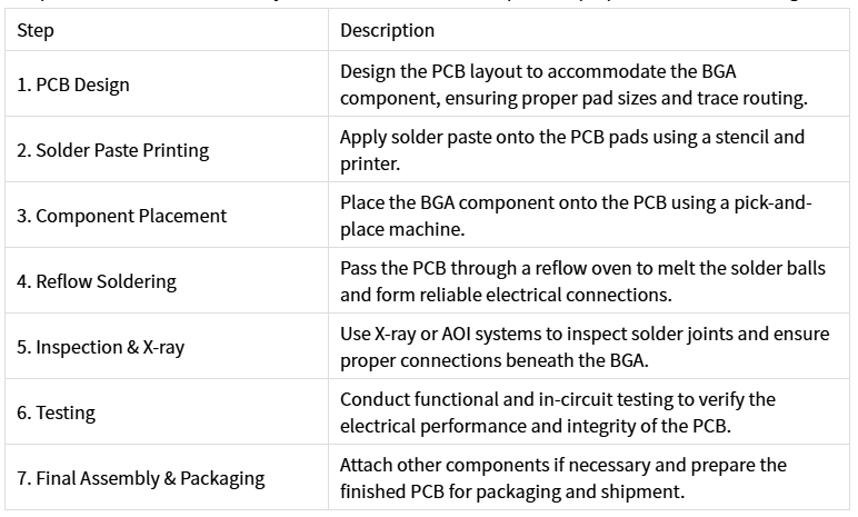
The process of BGA PCB assembly involves several critical steps, from preparation to final testing. Here’s a breakdown of the typical process:

BGA has several advantages over other packaging methods, which is why it’s widely used in modern electronics. Some key benefits include:
High Pin Count: BGA allows for a high density of connections in a compact form factor. This is particularly important in devices with limited space, such as smartphones or wearable technology.
Improved Signal Integrity: Because the solder balls are arranged in a grid pattern underneath the chip, the electrical paths are shorter and more uniform, leading to better signal integrity and performance.
Reduced Package Size: BGA components are smaller than traditional leaded components, allowing for greater miniaturization of devices.
Enhanced Thermal Performance: BGA packages are better at distributing heat compared to other packaging types, improving the overall thermal performance of the device.
Increased Reliability: The absence of leads reduces the risk of mechanical failure, and the use of solder balls ensures strong, reliable electrical connections.
While BGA packaging offers many benefits, it also presents challenges:
Complex Assembly Process: Assembling BGA packages requires precision and advanced equipment. The reflow soldering process and the need for X-ray inspection can make BGA assembly more complex and costly compared to traditional SMT assembly.
BGA Misalignment: During the placement of the BGA component, any misalignment of the solder balls on the pads can cause poor connections or even failure of the PCB.
Inspection Difficulty: Traditional visual inspection methods do not work well for BGA components because the solder joints are hidden underneath the package. This requires special inspection techniques, such as X-ray or AOI.
To ensure the success of BGA PCB assembly, there are several key factors to consider:
PCB Design: Ensure that the PCB layout is optimized for BGA components, with proper pad sizes, trace routing, and sufficient spacing to accommodate the BGA’s ball grid.
Soldering Process: Pay attention to the reflow profile and ensure that the soldering temperature is precisely controlled to avoid defects like cold joints or solder bridges.
Inspection: Utilize X-ray inspection or automated optical inspection (AOI) to detect hidden issues with the solder joints that could affect the performance of the device.
Testing: Conduct thorough functional and in-circuit testing to ensure that the PCB functions as expected and that all electrical connections are intact.
BGA PCB assembly is an advanced process that plays a vital role in producing high-performance electronic devices. By leveraging the benefits of BGA packaging, companies can achieve higher-density designs, better signal integrity, and improved reliability. However, BGA assembly requires careful planning, precision in soldering, and advanced inspection techniques to ensure that the final product meets quality standards. Understanding the complexities and challenges involved in BGA PCB assembly can help businesses make informed decisions, leading to successful product development and manufacturing.
China BGA PCB assembly offers an ideal solution for companies seeking high-quality, cost-effective manufacturing for their electronic products. With advanced technology, skilled labor, and a robust supply chain, China excels in delivering precise BGA assembly services that meet global standards. The country’s expertise in handling complex BGA designs, combined with its competitive pricing, makes it a top choice for businesses looking to scale production without compromising on quality. Choosing China for BGA PCB assembly ensures reliability, efficiency, and timely delivery, making it a preferred destination for global electronics manufacturers.
